Product Introduction:AIM7
Overview
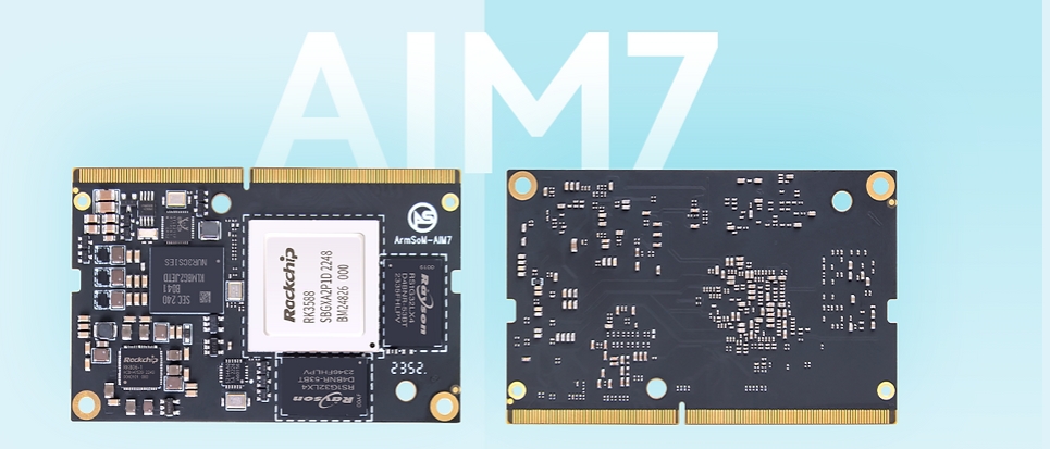
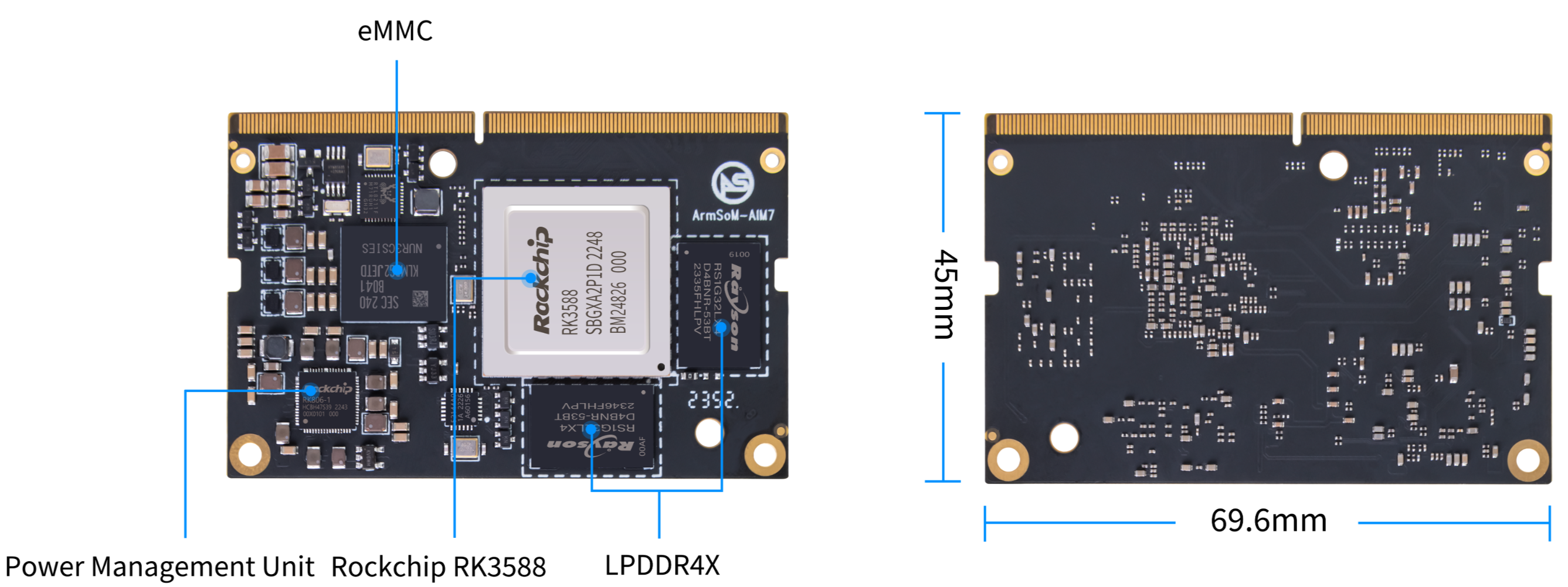
ArmSoM-AIM7 uses Rockchip RK3588, a new generation flagship eight-core 64-bit processor with a main frequency of up to 2.4GHz, 6 TOPS computing power NPU, and can be equipped with up to 32GB of large memory. While the interface is fully compatible with Jetson Nano, the PCIe interface has been upgraded to PCIe3.0 4-lane and PCIe2.1 1-lan.
AIM7 can be applied to ARM PC, edge computing, cloud server, artificial intelligence, cloud computing, virtual/augmented reality, blockchain, smart NVR and other fields
Key Parameters
- SOC: Rockchip RK3588
- CPU: RK3588 quad-core Cortex-A76 @ 2.4GHz + quad-core Cortex-A55 @ 1.8GHz, 8nm process
- GPU: ARM Mali-G610 MP4
- NPU: Computing power up to 6 TOPS (INT8), supports INT4/INT8/INT16 mixed computing
- VPU/Codec:
- Hardware decoding: 8K@60fps H.265/VP9/AVS2, 8K@30fps H.264 AVC/MVC, 4K@60fps AV1, 1080P@60fps MPEG-2/-1/VC-1/VP8
- Hardware encoding: 8K@30fps H.265 / H.264
- RAM: 8GB/16GB/32GB (max 32GB) 64bit LPDDR4x, default LPDDR4x 8GB
- Flash: 32GB/64GB/128GB eMMC, default eMMC 32GB
- Interface type: 260pin SO-DIMM connector, compatible with Jetson TX2 NX
- Working voltage: 5V DC
- Temperature: Operating temperature: 0°C to 80°C, Storage temperature: -20°C to 85°C
- Humidity: Relative humidity: Operation: 10% to 90%, Storage: 5% to 95%
- operating system:
- Rockchip official support: Android 12.0, Debian11, Buildroot
- Third-party support: Armbian 23.07, Ubuntu 20.04, Ubuntu22.04, Kylin OS
- PCB: 12-layer PCB board design
- weight:
- Size: 69.6 mm x 45 mm
Hardware
Hardware Interface
All pins of AIM7 are compatible with NVIDIA Jetson TX2 & NVIDIA Jetson Nano, with the same dimensions
Hardware Specification
| Specifications | ArmSoM-AIM7(Rockchip) | Jetson Nano (NVIDIA) |
|---|---|---|
| CPU Cores | Quad-core ARM® Cortex®-A76 + Quad-core ARM®Cortex®-A55 | Quad-core ARM® Cortex®-A57 MPCore processor |
| GPU Cores | ARM Mali-G610 MP4 | 128-core Maxwell GPU |
| Memory | 8GB/32GB 64-bit LPDDR4x, 2112MHz | 4GB 64-bit LPDDR4, 1600MHz |
| Storage | microSD card, 32GB eMMC 5.1 flash storage | microSD card, 16GB eMMC 5.1 flash storage |
| Video Encoding | 8K@30fps H.265 / H.264 | 250 MP/sec, 1x 4K@30 (HEVC), 2x 1080p@60 (HEVC), 4x 1080p@30 (HEVC) |
| Video Decoding | 8K@60fps H.265/VP9/AVS2, 8K@30fps H.264 AVC/MVC, 4K@60fps AV1, 1080P@60fps MPEG-2/-1/VC-1/VP8 | 500 MP/s, 1x 4K@60 (HEVC), 2x 4K@30 (HEVC), 4x 1080p@60 (HEVC), 8x 1080p@30 (HEVC) |
| USB Ports | 1 USB 3.0, 3 USB 2.0 | 1 USB 3.0, 3 USB 2.0 |
| Ethernet | 1 10/100/1000 BASE-T | 1 10/100/1000 BASE-T |
| CSI Interfaces | 12 channels (4x2) MIPI CSI-2 D-PHY1.1 (18 Gbps) | 12 channels (3x4 or 4x2) MIPI CSI-2 D-PHY 1.1 (18 Gbps) |
| I/O | 3 UARTs, 2 SPIs, 2 I2S, 4 I2Cs, multiple GPIOs | 3 UARTs, 2SPIs, 2 I2S, 4 I2Cs, multiple GPIOs |
| PCIE | 1 1/2/4lane PCIE3.0 & 1 1lane PCIE2.0 | 1 1/2/4lane PCIE2.0 |
| HDMI Output | 1 HDMI OUT2.1 / 1 eDP 1.4 | 1 HDMI 2.0 |
| DP Interface | 1 DP1.4a | 1 DP1.2 |
| eDP/DP Interface | 1 eDP 1.4 / 1 HDMI OUT2.1 | 1 eDP 1.4 / 1 DP |
| DSI Interface | 1 DSI (1 x2) 2 sync | 1 DSI (1 x2) 2 sync |
| OS Support | Support debian, ubuntu, armbian, kernel 5.10 | NVIDIA JetPack software suite |
| Size | 69.6 mm x 45 mm | 69.6 mm x 45 mm |
| Form Factor | 260-pin edge connector | 260-pin edge connector |
Hardware Pin Definitions
Video input interface
Two MIPI DC (DPHY/CPHY) combo PHY
- Support USE DPHY or CPHY
- Each MIPI DPHY V2.0, 4 lanes, 4.5 Gbps per lane
- Each MIPI CPHY V1.1, 3 lanes, 2.5 Gbps per lane
Four MIPI CSI DPHY
- Each MIPI DPHY V1.2, 2 lanes, 2.5 Gbps per lane
- Support combine 2 DPHY together to one 4-lan
Table 1. CSI0 pin descriptions
| Pin | Pin name | Signal description | Direction | Pin type |
|---|---|---|---|---|
| 2 | GND | Ground | ||
| 4 | CSI0_D0_N | Camera, CSI 0 Data 0– | Input | MIPI D-PHY |
| 6 | CSI0_D0_P | Camera, CSI 0 Data 0 | + Input | MIPI D-PHY |
| 8 | GND | Ground | ||
| 10 | CSI0_CLK_N | Camera, CSI 0 Clock– | Input | MIPI D-PHY |
| 12 | CSI0_CLK_P | Camera, CSI 0 Clock+ | Input | MIPI D-PHY |
| 14 | GND | Ground | ||
| 16 | CSI0_D1_N | Camera, CSI 0 Data 1– | Input | MIPI D-PHY |
| 18 | CSI0_D1_P | Camera, CSI 0 Data 1+ | Input | MIPI D-PHY |
| 114 | CAM0_PWDN | Camera, CSI 0 Data 1– | Input | MIPI D-PHY |
| 116 | CAM0_MCLK | Camera, CSI 0 Data 1+ | Input | MIPI D-PHY |
Table 2. CSI1 pin descriptions
| Pin | Pin name | Signal description | Direction | Pin type |
|---|---|---|---|---|
| 1 | GND | Ground | ||
| 3 | MIPI_CSI0_RX_D2N | Camera, CSI 1 Data 0– | Input | MIPI D-PHY |
| 5 | MIPI_CSI0_RX_D2P | Camera, CSI 1 Data 0+ | Input | MIPI D-PHY |
| 7 | GND | Ground | ||
| 9 | CSI1_CLK_N | Camera, CSI 1 Clock– | Input | MIPI D-PHY |
| 11 | CSI1_CLK_P | Camera, CSI 1 Clock+ | Input | MIPI D-PHY |
| 15 | CSI1_D1_N | Camera, CSI 1 Data 1– | Input | MIPI D-PHY |
| 17 | CSI1_D1_P | Camera, CSI 1 Data 1+ | Input | MIPI D-PHY |
| 118 | CAM1_PWDN | Camera, CSI 0 Data 1– | Input | MIPI D-PHY |
| 126 | CAM1_MCLK | Camera, CSI 0 Data 1+ | Input | MIPI D-PHY |
Table 3. CSI2 pin descriptions
| Pin | Pin name | Signal description | Direction | Pin type |
|---|---|---|---|---|
| 20 | GND | Ground | ||
| 22 | CSI2_D0_N | Camera, CSI 2 Data 0– | Input | MIPI D-PHY |
| 24 | CSI2_D0_P | Camera, CSI 2 Data 0+ | Input | MIPI D-PHY |
| 26 | GND | Ground | ||
| 28 | CSI2_CLK_N | Camera, CSI 2 Clock– | Input | MIPI D-PHY |
| 30 | CSI2_CLK_P | Camera, CSI 2 Clock+ | Input | MIPI D-PHY |
| 32 | GND | Ground | ||
| 34 | CSI2_D1_N | Camera, CSI 2 Data 1– | Input | MIPI D-PHY |
| 36 | CSI2_D1_P | Camera, CSI 2 Data 1+ | Input | MIPI D-PHY |
| 120 | CAM2_MCLK | Camera, CSI 2 Data 1– | Input | MIPI D-PHY |
| 122 | CAM2_PWDN | Camera, CSI 2 Data 1+ | Input | MIPI D-PHY |
Table 3. CSI3 pin descriptions
| Pin | Pin name | Signal description | Direction | Pin type |
|---|---|---|---|---|
| 19 | GND | Ground | ||
| 21 | CSI3_D0_N | Camera, CSI 3 Data 0– | Input | MIPI D-PHY |
| 23 | CSI3_D0_P | Camera, CSI 3 Data 0+ | Input | MIPI D-PHY |
| 25 | GND | Ground | ||
| 27 | CSI3_CLK_N | Camera, CSI 3 Clock– | Input | MIPI D-PHY |
| 29 | CSI3_CLK_P | Camera, CSI 3 Clock+ | Input | MIPI D-PHY |
| 31 | GND | Ground | ||
| 33 | CSI3_D1_N | Camera, CSI 3 Data 1– | Input | MIPI D-PHY |
| 35 | CSI3_D1_P | Camera, CSI 3 Data 1+ | Input | MIPI D-PHY |
| 216 | CAM3_MCLK | Camera, CSI 3 Data 1– | Input | MIPI D-PHY |
| 218 | CAM3_PWDN | Camera, CSI 3 Data 1+ | Input | MIPI D-PHY |
Table 4. CSI4 pin descriptions
| Pin | Pin name | Signal description | Direction | Pin type |
|---|---|---|---|---|
| 38 | GND | Ground | ||
| 40 | CSI4_D2_N | Camera, CSI 4 Data 2– | Input | MIPI D/C-PHY |
| 42 | CSI4_D2_P | Camera, CSI 4 Data 2+ | Input | MIPI D/C-PHY |
| 44 | GND | Ground | ||
| 52 | CSI4_CLK_N | Camera, CSI 4 Clock– | Input | MIPI D/C-PHY |
| 54 | CSI4_CLK_P | Camera, CSI 4 Clock+ | Input | MIPI D/C-PHY |
| 46 | CSI4_D0_N | Camera, CSI 4 Data 0– | Input | MIPI D/C-PHY |
| 48 | CSI4_D0_P | Camera, CSI 4 Data 0+ | Input | MIPI D/C-PHY |
| 58 | CSI4_D1_N | Camera, CSI 4 Data 1– | Input | MIPI D/C-PHY |
| 60 | CSI4_D1_P | Camera, CSI 4 Data 1+ | Input | MIPI D/C-PHY |
| 64 | CSI4_D3_N | Camera, CSI 4 Data 3– | Input | MIPI D/C-PHY |
| 66 | CSI4_D3_P | Camera, CSI 4 Data 3+ | Input | MIPI D/C-PHY |
| 228 | CAM4_MCLK | Camera, CSI 4 Data 1– | Input | MIPI D-PHY |
| 230 | CAM4_PWDN | Camera, CSI 4 Data 1+ | Input | MIPI D-PHY |
Video output processor
HDMI/eDP TX interface
- Support x1, x2 and x4 configuration for each interface
- Support all the data rates for HDMI FRL: 3, 6, 8, 10 and 12Gbps
- Support 1.62Gbps, 2.7Gbps and 5.4Gbps for eDP
- Support up to 7680x4320@60Hz for HDMI TX, and 4K@60Hz for eDP
- Support RGB/YUV(up to 10bit) format for HDMI TX
- Support RGB, YCbCr 4:4:4, YCbCr 4:2:2 and 8/10 bit per component video format for eDP
- Support DSC 1.2a for HDMI TX
- Support HDCP2.3 for HDMI TX, and HDCP1.3 for eDP
DP TX interface
- Support 2 DP TX 1.4a interface which combo with USB3.1 Gen1
- Support 1/2/4lanes for each interface
- Support 1.62Gbps, 2.7Gbps, 5.4Gbps and 8.1Gbps Serializer
- Support up to 7680x4320@30Hz
- Support RGB/YUV(up to 10bit) format
- Support Single Stream Transport(SST)
- Support DP Alt mode on USB Type-C
- Support HDCP2.3, HDCP 1.3
MIPI DSI interface
- Support 2 MIPI DPHY 2.0 interfaces
- Support 4 data lanes and 4.5 Gbps maximum data rate per lane
- Support max resolution 4K@60 Hz
- Support dual MIPI display: left-right mode
- Support RGB (up to 10 bits) format
- Support DSC 1.1/1.2a
Table 5. DSI pin descriptions
| Pin | Pin name | Signal description | Direction | Pin type |
|---|---|---|---|---|
| 68 | GND | Ground | ||
| 70 | DSI_D0_N | DSI Data 0– | Output | MIPI D-PHY |
| 72 | DSI_D0_P | DSI Data 0+ | Output | MIPI D-PHY |
| 74 | GND | Ground | ||
| 76 | DSI_CLK_N | DSI Clock– | Output | MIPI D-PHY |
| 78 | DSI_CLK_P | DSI Clock+ | Output | MIPI D-PHY |
| 80 | GND | Ground | ||
| 82 | DSI_D1_N | DSI Data 1– | Output | MIPI D-PHY |
| 84 | DSI_D1_P | DSI Data 1+ | Output | MIPI D-PHY |
Table 6. DP / USB3.0 pin descriptions
| Pin | Pin name | Signal description | Direction | Pin type |
|---|---|---|---|---|
| 37 | GND | Ground | ||
| 39 | DP0_TXD0_N | Display Port 0 Lane 0- | Output | DP |
| 41 | DP0_TXD0_P | Display Port 0 Lane 0+ | Output | DP |
| 43 | GND | Ground | ||
| 45 | DP0_TXD1_N | Display Port 0 Lane 1– | Output | DP |
| 47 | DP0_TXD1_P | Display Port 0 Lane 1+ | Output | DP |
| 49 | GND | Ground | ||
| 51 | DP0_TXD2_N | Display Port 0 Lane 2– | Output | DP |
| 53 | DP0_TXD2_P | Display Port 0 Lane 2+ | Output | DP |
| 55 | GND | Ground | ||
| 57 | DP0_TXD3_N | Display Port 0 Lane 3– | Output | DP |
| 59 | DP0_TXD3_P | Display Port 0 Lane 3+ | Output | DP |
| 86 | GND | Ground | ||
| 88 | DP0_HPD | Display Port 0 Hot Plug Detect | Input | Open Drain–1.8V |
| 90 | DP0_AUX_N | Display Port 0 Aux– | Bidir | DP |
| 92 | DP0_AUX_P | Display Port 0 Aux+ | Bidir | DP |
Table 7. eDP/HDMI pin descriptions
| Pin | Pin name | Signal description | Direction | Pin type |
|---|---|---|---|---|
| 61 | GND | Ground | ||
| 63 | HDMI_TXD2_N/EDP_TX0_D2N | HDMI/EDP Lane 2– | Output | HDMI/EDP |
| 65 | HDMI_TXD2_P/EDP_TX0_D2P | HDMI/EDP Lane 2+ | Output | HDMI/EDP |
| 67 | GND | Ground | ||
| 69 | HDMI_TXD1_N/EDP_TX0_D1N | HDMI/EDP Lane 1– | Output | HDMI/EDP |
| 71 | HDMI_TXD1_P/EDP_TX0_D1P | HDMI/EDP Lane 1+ | Output | HDMI/EDP |
| 73 | GND | Ground | ||
| 75 | HDMI_TXD0_N/EDP_TX0_D0N | HDMI/EDP Lane 0– | Output | HDMI/EDP |
| 77 | HDMI_TXD0_P/EDP_TX0_D0P | HDMI/EDP Lane 0+ | Output | HDMI/EDP |
| 79 | GND | Ground | ||
| 81 | HDMI_CLK_N/EDP_TX0_D3N | HDMI/EDP Clk Lane– | Output | HDMI/EDP |
| 83 | HDMI_CLK_P/EDP_TX0_D3P | HDMI/EDP Clk Lane+ | Output | HDMI/EDP |
| 98 | HDMI_SDA / EDP_TX0_AUXN | HDMI/EDP DDC SDA | Bidir | Open-Drain,3.3V |
| 100 | HDMI_SCL / EDP_TX0_AUXP | HDMI/EDP DDC SCL | Output | Open-Drain,3.3V |
| 96 | HDMI_CEC | HDMI/EDP Hot Plug Detect | Input | Open Drain–3.3V |
| 94 | HDMI_HPD | HDMI/EDP CEC | Bidir | Open Drain–1.8V |
SDIO
- Compatible with SDIO3.0 protocol
- 4-bit data bus width
Table 8. SDIO pin descriptions
| Pin | Pin name | Signal description | Direction | Pin type |
|---|---|---|---|---|
| 217 | GND | Ground | ||
| 219 | SDMMC_DAT0 | SD Card or SDIO Data 0 | Bidir | CMOS – 1.8V/3.3V |
| 221 | SDMMC_DAT1 | SD Card or SDIO Data 1 | Bidir | CMOS – 1.8V/3.3V |
| 223 | SDMMC_DAT2 | SD Card or SDIO Data 2 | Bidir | CMOS – 1.8V/3.3V |
| 225 | SDMMC_DAT3 | SD Card or SDIO Data 3 | Bidir | CMOS – 1.8V/3.3V |
| 227 | SDMMC_CMD | SD Card or SDIO Command | Bidir | CMOS – 1.8V/3.3V |
| 229 | SDMMC_CLK | SD Card or SDIO Clock | Output | CMOS – 1.8V/3.3V |
| 126 | SDMMC_DET | SD Card or SDIO DET | Output | CMOS – 1.8V/3.3V |
GMAC
Table 9. Gigabit Ethernet pin descriptions
| Pin | Pin name | Signal description | Direction | Pin type |
|---|---|---|---|---|
| 184 | GBE_MDI0_N | GbE Transformer Data 0– | Bidir | MDI |
| 186 | GBE_MDI0_P | GbE Transformer Data 0+ | Bidir | MDI |
| 188 | GBE_LED_LINK | Ethernet Link LED (Green) | Output | - |
| 190 | GBE_MDI1_N | GbE Transformer Data 1– | Bidir | MDI |
| 192 | GBE_MDI1_P | GbE Transformer Data 1+ | Bidir | MDI |
| 194 | GBE_LED_ACT | Ethernet Activity LED (Yellow) | Output | - |
| 196 | GBE_MDI2_N | GbE Transformer Data 2– | Bidir | MDI |
| 198 | GBE_MDI2_P | GbE Transformer Data 2+ | Bidir | MDI |
| 200 | GND | Ground | ||
| 202 | GBE_MDI3_N | GbE Transformer Data 3– | Bidir | MDI |
| 204 | GBE_MDI3_P | GbE Transformer Data 3+ | Bidir | MDI |
USB3.0
- Embedded two USB 3.0 OTG interfaces which combo with DP TX (USB3OTG_0 and USB3OTG_1)
- Embedded one USB 3.0 Host interface which combos with Combo PIPE PHY2 (USB3OTG_2)
Table 10. USB 3.0 GEN1 pin descriptions
| Pin | Pin name | Signal description | Direction | Pin type |
|---|---|---|---|---|
| 113 | GND | Ground | ||
| 161 | PCIE20_2_RXN/SATA30_2_RXN/USBSS_RX_N | USB SS Receive- (USB 3.0 Ctrl #0) | Input | USB SS PHY |
| 163 | PCIE20_2_RXP/SATA30_2_RXP/USBSS_RX_P | USB SS Receive+ (USB 3.0 Ctrl #0) | Input | USB SS PHY |
| 166 | PCIE20_2_TXN/SATA30_2_TXN/USBSS_TX_N | USB SS Transmit- (USB 3.0 Ctrl #0) | Output | USB SS PHY |
| 168 | PCIE20_2_TXP/SATA30_2_TXP/USBSS_TX_P | USB SS Transmit+ (USB 3.0 Ctrl #0) | Output | USB SS PHY |
USB 2.0 Host
- Compatible with USB 2.0 specification
- Support two USB 2.0 Hosts
- Supports high-speed (480 Mbps), full-speed (12 Mbps) and low-speed (1.5 Mbps) mode
- Support Enhanced Host Controller Interface Specification (EHCI), Revision 1.0
- Support Open Host Controller Interface Specification (OHCI), Revision 1.0a
Table 11. USB 2.0 pin descriptions
| Pin | Pin name | Signal description | Direction | Pin type |
|---|---|---|---|---|
| 109 | USB0_D_N | USB2.0 Port 0 Data– | Bidir | USB PHY |
| 111 | USB0_D_P | USB2.0 Port 0 Data+ | Bidir | USB PHY |
| 115 | USB1_D_N | USB 2.0 Port 1 Data– | Bidir | USB PHY |
| 117 | USB1_D_P | USB 2.0 Port 1 Data+ | Bidir | USB PHY |
| 121 | USB2_D_N | USB 2.0 Port 2 Data– | Bidir | USB PHY |
| 123 | USB2_D_P | USB 2.0 Port 2 Data+ | Bidir | USB PHY |
PCIe
PCIe 2.1 interface
- Compatible with PCI Express Base Specification Revision 2.1
- Support one lane for each PCIe 2.1 interface
- Support Root Complex (RC) only
- Support 5 Gbps data rate
Table 12. PCIe 2.1 pin descriptions
| Pin | Pinname | Signal description | Direction | Pin type |
|---|---|---|---|---|
| 171 | GND | Ground | ||
| 173 | PCIE1_CLK_N | PCIe #1 Reference Clock– (PCIe Ctrl #2) | Output | PCIe PHY |
| 175 | PCIE1_CLK_P | PCIe #1 Reference Clock+ (PCIe Ctrl #2) | Output | PCIe PHY |
| 165 | GND | Ground | ||
| 167 | PCIE1_RX_N/SATA30_0_RXN | PCIe #1 Receive 0– (PCIe Ctrl #2 Lane 0) | Input | PCIe PHY |
| 169 | PCIE1_RX_P/SATA30_0_RXP | PCIe #1 Receive 0+ (PCIe Ctrl #2 Lane 0) | Input | PCIe PHY |
| 172 | PCIE1_TX_N | PCIe #1 Transmit 0– (PCIe Ctrl #2 Lane 0) | Output | PCIe PHY |
| 174 | PCIE1_TX_P | PCIe #1 Transmit 0+ (PCIe Ctrl #2 Lane 0) | Output | PCIe PHY |
| 124 | PCIE_20X1_2_WAKE | PCIe Wake. 47kΩ pull-up to 3.3V on themodule. | Input | Open Drain – 3.3V |
| 182 | PCIE_20X1_2_CLKREQ | PCIe #1 Clock Request (PCIe Ctrl #2). 47kΩ pull-up to 3.3V on the module. | Bidir | Open Drain – 3.3V |
| 183 | PCIE_20X1_2_RST | PCIe #1 Reset (PCIe Ctrl #2). 4.7kΩ pull-up to 3.3V on the module. | Output | Open Drain – 3.3V |
PCIe 3.0 interface
- Compatible with PCI Express Base Specification Revision 3.0
- Support dual operation modes: Root Complex (RC) and End Point (EP)
- Support data rates: 2.5 Gbps (PCIe 1.1), 5 Gbps (PCIe 2.1), 8 Gbps (PCIe 3.0)
- Support aggregation and bifurcation with 1x 4 lanes, 2x 2 lanes, 4x 1 lanes and 1x 2 lanes + 2x 1 lanes
Table 13. PCIe 3.0 pin descriptions
| Pin | Pin name | Signal description | Direction | Pin type |
|---|---|---|---|---|
| 158 | GND | Ground | ||
| 160 | PCIE0_CLK_N | PCIe #0 Reference Clock– | Output | PCIe PHY |
| 162 | PCIE0_CLK_P | PCIe #0 Reference Clock+ | Output | PCIe PHY |
| 129 | GND | Ground | ||
| 131 | PCIE0_RX0_N | PCIe #0 Receive 0– (PCIe Ctrl #0 Lane 0) | Input | PCIe PHY |
| 133 | PCIE0_RX0_P | PCIe #0 Receive 0+ (PCIe Ctrl #0 Lane 0) | Input | PCIe PHY |
| 132 | GND | Ground | ||
| 134 | PCIE0_TX0_N | PCIe #0 Transmit 0– (PCIe Ctrl #0 Lane 0) | Output | PCIe PHY |
| 136 | PCIE0_TX0_P | PCIe #0 Transmit 0+ (PCIe Ctrl #0 Lane 0) | Output | PCIe PHY |
| 177 | GND | Ground | ||
| 179 | PCIE_30X4_WAKE | PCIe Wake. 47kΩ pull-up to 3.3V on themodule. | Input | Open Drain – 3.3V |
| 180 | PCIE_30X4_CLKREQ | PCIe #0 Clock Request (PCIe Ctrl #0). 47kΩpull-up to 3.3V on the module. | Bidir | Open Drain – 3.3V |
| 181 | PCIE_30X4_RST | PCIe #0 Reset (PCIe Ctrl #0). 4.7kΩ pull-up to3.3V on the module. | Bidir | Open Drain – 3.3V |
| 135 | GND | Ground | ||
| 137 | PCIE0_RX1_N | PCIe #0 Receive 1– (PCIe Ctrl #0 Lane 1) | Input | PCIe PHY |
| 139 | PCIE0_RX1_P | PCIe #0 Receive 1+ (PCIe Ctrl #0 Lane 1) | Input | PCIe PHY |
| 138 | GND | Ground | ||
| 140 | PCIE0_TX1_N | PCIe #0 Transmit 1– PCIe Ctrl #0 Lane 1) | Output | PCIe PHY |
| 142 | PCIE0_TX1_P | PCIe #0 Transmit 1+ (PCIe Ctrl #0 Lane 1) | Output | PCIe PHY |
| 125 | GND | Ground | ||
| 127 | PCIE_30X1_0_WAKE | PCIe Wake. 47kΩ pull-up to 3.3V on themodule. | Input | Open Drain – 3.3V |
| 212 | PCIE_30X1_0_CLKREQ | PCIe #0 Clock Request (PCIe Ctrl #0). 47kΩpull-up to 3.3V on the module. | Bidir | Open Drain – 3.3V |
| 195 | PCIE_30X1_0_RST | PCIe #0 Reset (PCIe Ctrl #0). 4.7kΩ pull-up to3.3V on the module. | Bidir | Open Drain – 3.3V |
| 147 | GND | Ground | ||
| 149 | PCIE0_RX2_N | PCIe #0 Receive 2– (PCIe Ctrl #0 Lane 1) | Input | PCIe PHY |
| 151 | PCIE0_RX2_P | PCIe #0 Receive 2+ (PCIe Ctrl #0 Lane 1) | Input | PCIe PHY |
| 144 | GND | Ground | ||
| 146 | GND | Ground | ||
| 148 | PCIE0_TX2_N | PCIe #0 Transmit 2– PCIe Ctrl #0 Lane 1) | Output | PCIe PHY |
| 150 | PCIE0_TX2_P | PCIe #0 Transmit 2+ (PCIe Ctrl #0 Lane 1) | Output | PCIe PHY |
| 130 | PCIE_30X2_WAKE | PCIe Wake. 47kΩ pull-up to 3.3V on themodule. | Input | Open Drain – 3.3V |
| 120 | PCIE_30X2_CLKREQ | PCIe #0 Clock Request (PCIe Ctrl #0). 47kΩpull-up to 3.3V on the module. | Bidir | Open Drain – 3.3V |
| 195128 | PCIE_30X2_RST | PCIe #0 Reset (PCIe Ctrl #0). 4.7kΩ pull-up to3.3V on the module. | Bidir | Open Drain – 3.3V |
| 153 | GND | Ground | ||
| 155 | PCIE0_RX3_N | PCIe #0 Receive 3– (PCIe Ctrl #0 Lane 1) | Input | PCIe PHY |
| 157 | PCIE0_RX3_P | PCIe #0 Receive 3+ (PCIe Ctrl #0 Lane 1) | Input | PCIe PHY |
| 152 | GND | Ground | ||
| 154 | PCIE0_TX3_N | PCIe #0 Transmit 3– PCIe Ctrl #0 Lane 1) | Output | PCIe PHY |
| 156 | PCIE0_TX3_P | PCIe #0 Transmit 3+ (PCIe Ctrl #0 Lane 1) | Output | PCIe PHY |
| 199 | PCIE_30X1_1_WAKE | PCIe Wake. 47kΩ pull-up to 3.3V on themodule. | Input | Open Drain – 3.3V |
| 211 | PCIE_30X1_1_CLKREQ | PCIe #0 Clock Request (PCIe Ctrl #0). 47kΩpull-up to 3.3V on the module. | Bidir | Open Drain – 3.3V |
| 197 | PCIE_30X1_1_RST | PCIe #0 Reset (PCIe Ctrl #0). 4.7kΩ pull-up to3.3V on the module. | Bidir | Open Drain – 3.3V |
SPI interface
- Support 5 SPI Controllers (SPI0-SPI4)
- Support two chip-select output
- Support serial-master and serial-slave mode, software-configurable
Table 14. SPI pin descriptions
| Pin | Pin name | Signal description | Direction | Pin type |
|---|---|---|---|---|
| 89 | SPI0_MOSI | SPI 0 Master Out / Slave In | Bidir | CMOS – 1.8 |
| 91 | SPI0_SCK | SPI 0 Clock | Bidir | CMOS – 1.8 |
| 93 | SPI0_MISO_M2 | SPI 0 Master In / Slave Out | Bidir | CMOS – 1.8 |
| 95 | SPI0_CS0 | SPI 0 Chip Select 0 | Bidir | CMOS – 1.8 |
| 97 | SPI0_CS1 | SPI 0 Chip Select 1 | Bidir | CMOS – 1.8 |
| 102 | GND | Ground | ||
| 104 | SPI1_MOSI | SPI 1 Master Out / Slave In | Bidir | CMOS – 1.8 |
| 106 | SPI1_SCK | SPI 1 Clock | Bidir | CMOS – 1.8 |
| 108 | SPI1_MISO | SPI 1 Master In / Slave Out | Bidir | CMOS – 1.8 |
| 110 | SPI1_CS0 | SPI 1 Chip Select 0 | Bidir | CMOS – 1.8 |
| 112 | SPI1_CS1 | SPI 1 Chip Select 1 | Bidir | CMOS – 1.8 |
I2C interface
Table 15. I2C pin descriptions
| Pin | Pin name | Signal description | Direction | Pin type |
|---|---|---|---|---|
| 185 | I2C0_SCL | General I2C 0 Clock. 2.2kΩ pull-up to3.3V on module. | Bidir | Open Drain – 3.3V |
| 187 | I2C0_SDA | General I2C 0 Data. 2.2kΩ pull-up to 3.3V on the module. | Bidir | Open Drain – 3.3V |
| 189 | I2C1_SCL | General I2C 1 Clock. 2.2kΩ pull-up to 3.3V on the module. | Bidir | Open Drain – 3.3V |
| 191 | I2C1_SDA | General I2C 1 Data. 2.2kΩ pull-up to 3.3V on the module. | Bidir | Open Drain – 3.3V |
| 232 | I2C2_SCL | General I2C 2 Clock. 2.2kΩ pull-up to1.8V on the module. | Bidir | Open Drain – 1.8V |
| 234 | I2C2_SDA | General I2C 2 Data. 2.2kΩ pull-up to 1.8V on the module. | Bidir | Open Drain – 1.8V |
| 213 | CAM_I2C_SCL | Camera I2C Clock. 2.2kΩ pull-up to 3.3V on the module. | Bidir | Open Drain – 3.3V |
| 215 | CAM_I2C_SDA | Camera I2C Data. 2.2kΩ pull-up to 3.3V on the module. | Bidir | Open Drain – 3.3V |
UART interface
- Support 10 UART interfaces (UART0-UART9)
- Embedded two 64-byte FIFO for TX and RX operation respectively
- Support transmitting or receiving 5-bit, 6-bit, 7-bit, and 8-bit serial data
- Standard asynchronous communication bits such as start, stop and parity
- Support different input clocks for UART operation to get up to 4 Mbps baud rate
- Support auto flow control mode for all UART interfaces
Table 16. UART pin descriptions
| Pin | Pin name | Signal description | Direction | Pin type |
|---|---|---|---|---|
| 99 | UART0_TXD | UART #0 Transmit | Output | CMOS – 1.8V |
| 101 | UART0_RXD | UART #0 Receive | Input | CMOS – 1.8V |
| 103 | UART0_RTS | UART #0 Request to Send | Output | CMOS – 1.8V |
| 105 | UART0_CTS | UART #0 Clear to Send | Input | CMOS – 1.8V |
| 201 | GND | Ground | ||
| 203 | UART1_TXD | UART #1 Transmit | Output | CMOS – 1.8V |
| 205 | UART1_RXD | UART #1 Receive | Input | CMOS – 1.8V |
| 207 | UART1_RTS | UART #1 Request to Send | Output | CMOS – 1.8V |
| 209 | UART1_CTS | UART #1 Clear to Send | Input | CMOS – 1.8V |
| 236 | UART2_TXD | UART #2 Transmit | Output | CMOS – 1.8V |
| 238 | UART2_RXD | UART #2 Receive | Input | CMOS – 1.8V |
CAN bus
- Support transmitting or receiving CAN standard frame
- Support transmitting or receiving CAN extended frame
- Support transmitting or receiving data frame, remote frame, overload frame, error frame, and frame interval
Table 14. CAN pin descriptions
| Pin | Pin name | Signal description | Direction Pin type | |
|---|---|---|---|---|
| 141 | GND | Ground | ||
| 145 | CAN_TX | CAN PHY | Output | CMOS – 3.3V |
| 143 | CAN_RX | CAN PHY | Input | CMOS – 3.3V |
GPIO
- All GPIOs can be used to generate interrupt
- Support level trigger and edge trigger interrupt
- Support configurable polarity of level trigger interrupt
- Support configurable rising edge, falling edge and both edge trigger interrupt
- Support configurable pull direction (a weak pull-up and a weak pull-down)
- Support configurable drive strength
Table 15. GPIO pin descriptions
| Pin | Pin name | Signal description | Direction | Pin type |
|---|---|---|---|---|
| 87 | GPIO0/GPIO1_C5/VBUS_DET | GPIO #0 or USB 0 VBUS Enable #0 | Bidir | CMOS – 1.8V |
| 118 | GPIO01/GPIO3_A7/CAM1_PWDN | GPIO #1 or Generic Clocks | Bidir | CMOS – 1.8V |
| 124 | GPIO02/GPIO3_A3/MIPI_CAM2_PDN | GPIO #2 | Bidir | CMOS – 1.8V |
| 126 | GPIO03/GPIO3_D0/PCIE20X1_2_WAKEN_M0 | GPIO #3 | Bidir | CMOS – 1.8V |
| 127 | GPIO04/GPIO4_A4/PCIE_30X1_0_WAKE | GPIO #4 | Bidir | CMOS – 1.8V |
| 128 | GPIO05/GPIO4_B0/PCIE30X2_PERSTN_M1 | GPIO #5 | Bidir | CMOS – 1.8V |
| 130 | GPIO06/GPIO4_A7/PCIE_30X2_WAKE | GPIO #6 | Bidir | CMOS – 1.8V |
| 206 | GPIO07/GPIO3_A0/PWM10 | GPIO #7 or Pulse Width Modulator | Bidir | CMOS – 1.8V |
| 208 | GPIO08/GPIO1_C6/PWM15_IR | GPIO #8 or Fan Tach | Bidir | CMOS – 1.8V |
| 211 | I2S1_MCLK_M0/PCIE30X1_1_CLKREQN_M1 | GPIO #9 or Audio Codec Master Clock | Bidir | CMOS – 1.8V |
| 212 | GPIO10/GPIO4_A3/PCIE_30X1_0_CLKREQ | GPIO #10 | Bidir | CMOS – 1.8V |
| 216 | GPIO11/GPIO3_B0/MIPI_CAM3_CLKOUT | GPIO #11 or Generic Clocks | Bidir | CMOS – 1.8V |
| 218 | GPIO12/I2S2_MCLK_M1/MIPI_CAM3_PDN | GPIO #12 or Pulse Width Modulator | Bidir | CMOS – 1.8V |
| 228 | GPIO13/GPIO3_B1/PWM2/MIPI_CAM4_CLKOUT | GPIO #13 or Pulse Width Modulator | Bidir | CMOS – 1.8V |
| 230 | GPIO14/GPIO3_A1/PWM11_IR/MIPI_CAM4_PDN | GPIO #14 or Pulse Width Modulator | Bidir | CMOS – 1.8V |
i2s interface
Table 16. i2s pin descriptions
| Pin | Pin name | Signal description | Direction | Pin type |
|---|---|---|---|---|
| 199 | I2S0_SCLK/PCIE_30X1_1_WAKE | I2S Audio Port 0 Clock | Bidir | CMOS – 1.8V |
| 197 | I2S0_FS/PCIE_30X1_1_RST | I2S Audio Port 0 Left/Right Clock | Bidir | CMOS – 1.8V |
| 193 | I2S0_DOUT | I2S Audio Port 0 Data Out | Output | CMOS – 1.8V |
| 195 | I2S0_DIN/PCIE_30X1_0_RST | I2S Audio Port 0 Data In | Input | CMOS – 1.8V |
| 226 | I2S1_SCLK | I2S Audio Port 1 Clock | Bidir | CMOS – 1.8V |
| 224 | I2S1_FS | I2S Audio Port 1 Left/Right Clock | Bidir | CMOS – 1.8V |
| 220 | I2S1_DOUT | I2S Audio Port 1 Data Out | Output | CMOS – 1.8V |
| 222 | I2S1_DIN | I2S Audio Port 1 Data In | Input | CMOS – 1.8V |
pin define
| ArmSoM-AIM7 function | Pin number | Pin number | ArmSoM-AIM7 function |
|---|---|---|---|
| GND_1 | 1 | 2 | GND_2 |
| CSI1_D0_N | 3 | 4 | CSI0_D0_N |
| CSI1_D0_P | 5 | 6 | CSI0_D0_P |
| GND_3 | 7 | 8 | GND_4 |
| CSI1_CLK_N | 9 | 10 | CSI0_CLK_N |
| CSI1_CLK_P | 11 | 12 | CSI0_CLK_P |
| GND_5 | 13 | 14 | GND_6 |
| CSI1_D1_N | 15 | 16 | CSI0_D1_N |
| CSI1_D1_P | 17 | 18 | CSI0_D1_P |
| GND_7 | 19 | 20 | GND_8 |
| CSI3_D0_N | 21 | 22 | CSI2_D0_N |
| CSI3_D0_P | 23 | 24 | CSI2_D0_P |
| GND_9 | 25 | 26 | GND_10 |
| CSI3_CLK_N | 27 | 28 | CSI2_CLK_N |
| CSI3_CLK_P | 29 | 30 | CSI2_CLK_P |
| GND_11 | 31 | 32 | GND_12 |
| CSI3_D1_N | 33 | 34 | CSI2_D1_N |
| CSI3_D1_P | 35 | 36 | CSI2_D1_P |
| GND_13 | 37 | 38 | GND_14 |
| TYPEC0_SSRX1N/DP0_TXD0_N | 39 | 40 | CSI4_D2_N |
| TYPEC0_SSRX1P/DP0_TXD0_P | 41 | 42 | CSI4_D2_P |
| GND_15 | 43 | 44 | GND_16 |
| TYPEC0_SSTX1N/DP0_TXD1_N | 45 | 46 | CSI4_D0_N |
| TYPEC0_SSTX1P/DP0_TXD1_P | 47 | 48 | CSI4_D0_P |
| GND_17 | 49 | 50 | GND_18 |
| TYPEC0_SSRX2N/DP0_TXD2_N | 51 | 52 | CSI4_CLK_N |
| TYPEC0_SSRX2P/DP0_TXD2_P | 53 | 54 | CSI4_CLK_P |
| GND_19 | 55 | 56 | GND_20 |
| TYPEC0_SSTX2N/DP0_TXD3_N | 57 | 58 | CSI4_D1_N |
| TYPEC0_SSTX2P/DP0_TXD3_P | 59 | 60 | CSI4_D1_P |
| GND_21 | 61 | 62 | GND_22 |
| HDMI_TXD2_N/EDP_TX0_D2N | 63 | 64 | CSI4_D3_N |
| HDMI_TXD2_P/EDP_TX0_D2P | 65 | 66 | CSI4_D3_P |
| GND_23 | 67 | 68 | GND_24 |
| HDMI_TXD1_N/EDP_TX0_D1N | 69 | 70 | DSI_D0_N |
| HDMI_TXD1_P/EDP_TX0_D1P | 71 | 72 | DSI_D0_P |
| GND_25 | 73 | 74 | GND_26 |
| HDMI_TXD0_N/EDP_TX0_D0N | 75 | 76 | DSI_CLK_N |
| HDMI_TXD0_P/EDP_TX0_D0P | 77 | 78 | DSI_CLK_P |
| GND_27 | 79 | 80 | GND_28 |
| HDMI_CLK_N/EDP_TX0_D3N | 81 | 82 | DSI_D1_N |
| HDMI_CLK_P/EDP_TX0_D3P | 83 | 84 | DSI_D1_P |
| GND_29 | 85 | 86 | GND_30 |
| GPIO0/GPIO1_C5/VBUS_DET | 87 | 88 | DP0_HPD |
| SPI0_MOSI | 89 | 90 | DP0_AUX_N |
| SPI0_SCK | 91 | 92 | DP0_AUX_P |
| SPI0_MISO_M2 | 93 | 94 | HDMI_HPD |
| SPI0_CS0 | 95 | 96 | HDMI_CEC |
| SPI0_CS1 | 97 | 98 | HDMI_SDA / EDP_TX0_AUXN |
| UART0_TXD | 99 | 100 | HDMI_SCL / EDP_TX0_AUXP |
| UART0_RXD | 101 | 102 | GND_31 |
| UART0_RTS | 103 | 104 | SPI1_MOSI |
| UART0_CTS | 105 | 106 | SPI1_SCK |
| GND_32 | 107 | 108 | SPI1_MISO |
| USB0_D_N | 109 | 110 | SPI1_CS0 |
| USB0_D_P | 111 | 112 | SPI1_CS1 |
| GND_33 | 113 | 114 | CAM0_PWDN |
| USB1_D_N | 115 | 116 | CAM0_MCLK |
| USB1_D_P | 117 | 118 | GPIO01/GPIO3_A7/CAM1_PWDN |
| GND_34 | 119 | 120 | CAM2_MCLK/PCIE30X2_CLKREQN_M1 |
| USB2_D_N | 121 | 122 | CAM2_PWDN |
| USB2_D_P | 123 | 124 | GPIO02/GPIO3_A3/MIPI_CAM2_PDN |
| GND_35 | 125 | 126 | GPIO03/GPIO3_D0/PCIE20X1_2_WAKEN_M0 |
| GPIO04/GPIO4_A4/PCIE_30X1_0_WAKE | 127 | 128 | GPIO05/GPIO4_B0/PCIE30X2_PERSTN_M1 |
| GND_36 | 129 | 130 | GPIO06/GPIO4_A7/PCIE_30X2_WAKE |
| PCIE0_RX0_N | 131 | 132 | GND_37 |
| PCIE0_RX0_P | 133 | 134 | PCIE0_TX0_N |
| GND_38 | 135 | 136 | PCIE0_TX0_P |
| PCIE0_RX1_N | 137 | 138 | GND_39 |
| PCIE0_RX1_P | 139 | 140 | PCIE0_TX1_N |
| GND_40 | 141 | 142 | PCIE0_TX1_P |
| CAN_RX | 143 | 144 | GND_41 |
| CAN_TX | 145 | 146 | GND_42 |
| GND_43 | 147 | 148 | PCIE0_TX2_N |
| PCIE0_RX2_N | 149 | 150 | PCIE0_TX2_P |
| PCIE0_RX2_P | 151 | 152 | GND_44 |
| GND_45 | 153 | 154 | PCIE0_TX3_N |
| PCIE0_RX3_N | 155 | 156 | PCIE0_TX3_P |
| PCIE0_RX3_P | 157 | 158 | GND_46 |
| GND_47 | 159 | 160 | PCIE0_CLK_N |
| PCIE20_2_RXN/SATA30_2_RXN/USBSS_RX_N | 161 | 162 | PCIE30_CLK_P |
| PCIE20_2_RXP/SATA30_2_RXP/USBSS_RX_P | 163 | 164 | GND_48 |
| GND_49 | 165 | 166 | PCIE20_2_TXN/SATA30_2_TXN/USBSS_TX_N |
| PCIE1_RX_N/SATA30_0_RXN | 167 | 168 | PCIE20_2_TXP/SATA30_2_TXP/USBSS_TX_P |
| PCIE1_RX_P/SATA30_0_RXP | 169 | 170 | GND_50 |
| GND_51 | 171 | 172 | PCIE1_TX_N/SATA30_0_TXN |
| PCIE1_CLK_N | 173 | 174 | PCIE1_TX_P/SATA30_0_TXP |
| PCIE1_CLK_P | 175 | 176 | GND_52 |
| GND_53 | 177 | 178 | MOD_SLEEP |
| PCIE_30X4_WAKE | 179 | 180 | PCIE_30X4_CLKREQ |
| PCIE_30X4_RST | 181 | 182 | PCIE_20X1_2_CLKREQ |
| PCIE_20X1_2_RST | 183 | 184 | GBE_MDI0_N |
| I2C0_SCL | 185 | 186 | GBE_MDI0_P |
| I2C0_SDA | 187 | 188 | GBE_LED_LINK |
| I2C1_SCL | 189 | 190 | GBE_MDI1_N |
| I2C1_SDA | 191 | 192 | GBE_MDI1_P |
| I2S0_DOUT | 193 | 194 | GBE_LED_ACT |
| I2S1_SDI0_M0/PCIE_30X1_0_RST | 195 | 196 | GBE_MDI2_N |
| I2S1_LRCK_M0/PCIE_30X1_1_RST | 197 | 198 | GBE_MDI2_P |
| I2S0_SCLK/PCIE_30X1_1_WAKE | 199 | 200 | GND_54 |
| GND_55 | 201 | 202 | GBE_MDI3_N |
| UART1_TXD | 203 | 204 | GBE_MDI3_P |
| UART1_RXD | 205 | 206 | GPIO07/GPIO3_A0/PWM10 |
| UART1_RTS | 207 | 208 | GPIO08/GPIO1_C6/PWM15_IR |
| UART1_CTS | 209 | 210 | 32KOUT |
| I2S1_MCLK_M0/PCIE30X1_1_CLKREQN_M1 | 211 | 212 | GPIO10/GPIO4_A3/PCIE_30X1_0_CLKREQ |
| CAM_I2C_SCL | 213 | 214 | RECOVERY_KEY |
| CAM_I2C_SDA | 215 | 216 | GPIO11/GPIO3_B0/MIPI_CAM3_CLKOUT |
| GND_56 | 217 | 218 | GPIO12/I2S2_MCLK_M1/MIPI_CAM3_PDN |
| SDMMC_DAT0 | 219 | 220 | I2S1_DOUT |
| SDMMC_DAT1 | 221 | 222 | I2S1_DIN |
| SDMMC_DAT2 | 223 | 224 | I2S1_FS |
| SDMMC_DAT3 | 225 | 226 | I2S1_SCLK |
| SDMMC_CMD | 227 | 228 | GPIO08 |
| SDMMC_CLK | 229 | 230 | GPIO14 |
| GND_57 | 231 | 232 | I2C2_SCL |
| SHUTDOWN_REQ | 233 | 234 | I2C2_SDA |
| PMIC_BBAT | 235 | 236 | UART2_TXD |
| POWER_EN | 237 | 238 | UART2_RXD |
| SYS_RESET | 239 | 240 | SLEEP/WAKE |
| GND | 241 | 242 | GND |
| GND | 243 | 244 | GND |
| GND | 245 | 246 | GND |
| GND | 247 | 248 | GND |
| GND | 249 | 250 | GNDs |
| VDD_IN | 251 | 252 | VDD_IN |
| VDD_IN | 253 | 254 | VDD_IN |
| VDD_IN | 255 | 256 | VDD_IN |
| VDD_IN | 257 | 258 | VDD_IN |
| VDD_IN | 259 | 260 | VDD_IN |
Resources
Source Code
Official Images
Third Party Systems
Hardware Resources
User Manual
Easy to buy sample
ArmSoM online shop: https://www.armsom.org/product-page/aim7
ArmSoM Aliexpress online shop: https://www.aliexpress.com/item/3256805434864544.html
ArmSoM Taobao shop: https://item.taobao.com/item.htm?id=714794342755
OEM&ODM, please contact: sales@armsom.org